14 April, 2013
Any frequent visitor to Counting On Currency would be well aware of the continuous game of development leap-frog between currency issuers and counterfeiters – but I am willing to bet none of them have heard of nanothentication. I should hope they haven’t heard the term – I think I just made it up – no matter if that is true, I think the terminology mashup makes sense… that said if you have followed recent developments in currency authentication features or the friendly competition between countries in the Currency Awards, you have probably seen examples of nanothentication.
Our good friends at Currency News have offered us the opportunity to repost their recent article (March 2013 Issue) featuring the technology of nanothentication, also known officially as High Speed Nanocrystallisation. Without the security advances available from technologies like High Speed Nanocrystallisation, the life expectancy of currency in general would be greatly influenced by hitech counterfeiters. Like many who cam before and have yet to be known, we owe these technologists and scientists a debt of gratitude for assuring our secure future – until the next leap-frog!
Next Phase of New Optically Variable Feature
Based on High Speed Nanocrystallisation
Researchers at the Lebedev Institute of Physics of the Russian Academy of Sciences in Moscow have developed a new technology that generates graphic designs with unique optically variable effects in the bulk of the substrate material. Their research is said to expand the range of optically variable devices currently available for banknotes, both paper and polymer, and is aimed at providing a simple, unambiguous and easy to verify public security feature.
Initial developments were first unveiled at the 9th Pan European High Security Printing Conference in St. Petersburg last year and targeted cotton-based substrates (see AN Vol 18, No 7), but is now available for polymer materials as well.
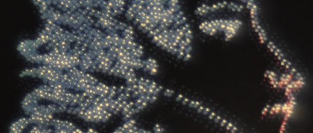
The core technology is based on short pulse laser interactions with matter and involves growing ordered nanostructures in the substrate material by exposing it to calculated laser radiation. In the case of paper, the substrate is first impregnated with a specially developed solution containing source material (metal salts) for nanostructure formations. Desired graphic designs are formed from resulting nanostructures, comprising a multitude of individual nanocrystals which are fused with the substrate in micro channels (50 μm-150 μm diameter), produced by laser-induced thermal energy.
The process of formation of the nanocrystal clusters occurs in just 10 nanoseconds  and has been subsequently characterised as high-speed nanocrystallisation in laser plasma. Despite high plasma temperatures of around 3500°C essential for crystal growth, the extremely short duration of the process prevents the paper from charring and allows embedding the structures in a matrix material without penetrating it all the way to the back.
  The fabricated images exhibit distinctive properties and can be used to authenticate a document on all levels – overt, covert and forensic examination. Their most distinguishing characteristic is unparalleled fluorescence in the UV spectrum. with an emission intensity higher than the amplitude of the fluorescence excitation spectrum, which is usually proportionate in UV inks and fibers.
Also Now for Polymer Materials
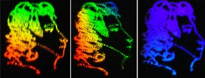
The technology has now been further developed for use on polymer-based substrates. In contrast to paper, where the metallic appearance is preserved regardless of the viewing angle, images formed in polymer-based materials display dynamic optical transitions. Rainbow-like spectral variations can be observed on tilting of the substrate in reflected light, while in transmitted light images remain monochrome and near-transparent in colour.
The effects stem from unusual properties and behaviour of crystals at nanoscale level and arise from confinement of the movement of electrons to small regions of space in three dimensions. With reductions in size down to tens of nanometers, the behaviour of individual atoms begins to dominate, changing the optical properties of crystals which absorb and emit light of a particular wavelength, depending on their size and orientation in the bulk material.
According to Prof Sergey Maximovsky and Grigory Radutsky, who have developed the technology and already own both Russian and international patents for its use on paper, the latest advances have the potential of taking optical sophistication in banknotes to a new level. The striking effects are easily recognisable, very simple to communicate but highly complex in their nature and consequently represent a serious barrier to counterfeiters.
The technology can be implemented either in the process of substrate production or as a film for stripes and threads with apertures, and the inventors are currently in discussion with several banknote printers about using both technologies in currency.


